
From Sand To Emojis
In times when things such as machine learning, sentient artificial intelligence and stable diffusion are on the hype, propelled by their undeniable potential but also by the opportunistic thrust of marketing departments, it is good to, every once in a while, connect back to what it all comes from. As I briefly walk on the beach in Noordwijk and I observe the unremarkable North Sea, I cannot help but thinking that it all still boils down to sand. But how so?
The sand we find on the beaches is mostly composed of silica, which is another name for silicon dioxide, or SiO2. Silica is one of the most complex and abundant families of materials, existing as a compound of several minerals. Silica is a crystalline material, which means that its atoms are linked in an orderly spatial lattice of silicon-oxygen tetrahedra, with each oxygen being shared between two adjacent tetrahedra.
Sand is abundant of silica and many other things, including macro particles as plastic and, say, dead fish. Then, SiO2 must be separated from all that stuff in order to be industrially used. How? Once all the macro impurities are removed, silica is melted in a furnace at high temperature and is reacted with carbon to produce silicon of a relative purity1.
Somewhere in 1915 a Polish scientist called Jan Czochralski woke up one morning on the wrong side of the bed and made a mistake: instead of dipping his pen into his inkwell, he dipped it in molten tin—why our Jan had molten tin on his desk is beyond me—and drew a tin filament, which later proved to be a single crystal. He had invented by accident a method which remains in use in most semiconductor industries around the world to grow silicon monocrystalline structures, which are manufactured as ingots that are then sliced into ultra-thin wafers that companies use to etch their integrated circuits layouts on. The process provides a proper, almost pure, monocrystalline silicon we can work with.
Crystals and their orderly structure have fascinated scientists for ages, perhaps due to the fact they provide an illusion of order and for that reason a relatively easier grasp of the underlying physics: condensed matter is a complex matter (hehe), but when it’s arranged in a more or less symmetrical manner in three dimensions, it may give the impression to be a tad simpler to comprehend. In a silicon crystal, each silicon atom forms four covalent bonds with four oxygen atoms, that is, each silicon atom sharing electrons with four oxygen atoms.
As we know, temperature is the quantitative measure of the kinetic energy of all particles that form a substance or material. In crystals, atoms do not really go anywhere but they vibrate in their fixed positions, as if they were wearing straitjackets. Temperature in crystalline structures indicates how violently atoms shake at their spots. Valence electrons, in thermal equilibrium with the crystal they belong to, share the kinetic energy with the rest of the material. But temperature tends to describe the average energy across the lattice. Momentary differences in local temperature may cause an electron to muster the guts to break its covalent bond and go solo. A bond without its precious electron is a broken bond, and as such will try to recover from this absence, so the affinity with neighboring electrons intensifies. If the broken bond manages to capture an electron from a neighboring bond, the problem is only passed to the neighbor, which will also soon pass it to the next one, and so on. The “hole” left behind by the initial emancipated electron spreads across the lattice. What happens with the initial fugitive electron? It travels across the lattice, emotionally disengaged from the problem it caused. Worth noting is that a broken bond creates two phenomena: a wandering hole, and a wandering free electron. Another way of calling such free electrons is conduction electrons.
Undisputed kings of negative charge, electrons leave positively charged zones behind them. Therefore, in the vicinity of holes, the charge is now more positive, and such positivity travels as the hole travels. Therefore, we can say holes have positive charge.
A wafer of pure monocrystalline silicon does not do much in and of itself. It is just an ‘intrinsic’ material with electrons and holes moving around because of bonds constantly being broken due to thermal agitation. Intrinsic materials create electron-hole pairs in exact numbers because one exists because of the other (along with some other particles existing inside intrinsic silicon as well, like photons). Intrinsic materials would be of little practical use if we couldn’t break the balance between electrons and holes. How to break that harmony? By opportunistically sprinkling our silicon crystals with more electrons (or more holes) by means of adding impurities. Didn’t we say impurities were bad? Yes, but these are more sophisticated, controlled impurities, unlike the microplastic that washes ashore on beaches as a product of our pointless mass consumption urges.
But here’s the issue: we cannot just add loose electrons like we add pepper to salad—the Coulomb forces would be insane due to the sudden electric charge imbalance. All we can do is to add atoms that can contribute with electrons, called donors. Examples of donors are phosphorus or arsenic. Typical proportions of impurity atoms is one of these guys for every million of silicon atoms.
When a donor atom is implanted in the lattice, it mimics the Si atom quite well: it completes the four covalent bonds the same way as Si atoms do. But arsenic happens to have 5 valence electrons, so one electron does not belong to any bond, and because it’s not trapped in any potential barrier, it has a higher energy than their other 4 cousins, and thus it has high chances of leaving the atom behind, leaving it positively charged, as a gift. An ion is born, fixed in the crystalline structure. A structure still remains electrically neutral at the macro level, but it’s now populated with positively charged spots, all balanced by the free electrons wandering around.
Conversely, acceptor impurities do the opposite. Aluminum, Indium and Gallium, for instance, are good examples of acceptor elements. Adding acceptors is a way of adding holes to a lattice, without breaking the macro electric neutrality. An Indium atom also fits itself comfortably in the lattice, replacing a Silicon atom, but it has only 3 valence electrons. You get the score. A hole is now there, because one covalent bond is missing. This vacant bond is open for business, and eventually it will get filled by an electron, breaking the impurity atom neutrality, and thus creating a negative ion.
In summary: impurities, whether donors or acceptors, will end up all being ionized. Donors will quickly lose an electron, and acceptors will quickly lose a hole (or gain an electron) because the energy to allow such ionization is quite low. Thermal agitation will make sure that practically all impurities will be ionized, therefore we can consider that all donors will lose their extra electron. This simplifies the math: we can estimate that the density of conduction electrons will be more or less equal to the density of donor atoms. The same goes for conduction holes. This way, a piece of silicon crystal with more donor impurities than acceptor impurities will be called type-n. Conversely, if more acceptors than donors are added to the silicon, the material will be called type-p. Conduction electrons and holes will not have it easy while traveling inside the lattice. Multiple things will alter their trajectories: repulsion forces coming from fellow moving carriers, un-ionized impurity atoms, ionized impurity atoms, and whatnot. Life of a charge carrier is not simple.
Now the magic starts to unfold when we sandwich type-n and type-p materials together. This is called a junction, and its properties are worth mentioning, because it sets the foundations of all solid state devices out there.
Junctions are not perfect; it is impossible to define a ideally abrupt boundary between a material partially doped with donors and partially with acceptors. Junctions can be more or less gradual, and this does not affect the physics behind them. It is very important to note that junctions are not made by welding one type-n crystal with a type-p crystal. A junction must still be made of a single crystal; there is no practical means of attaching together two bars of silicon with different impurities dosage and expect that it will work. The crystal lattice perfection is a key factor when it comes to junction’s performance.
In equilibrium (that is, with the piece of silicon that hosts the junction at some non zero temperature, and with no electric field applied), the concentration of acceptors will be maximum on the p-side, then decrease to zero as we approach the junction, and the same for donors on the n-side. With carriers moving due to the aforementioned thermal agitation, they cross the boundary thrusted by the gradient of impurities concentrations at the far ends. Holes come across the chasm and reach to the n-side, where they recombine easily because of the high density of electrons there. Conversely, electrons cross the boundary to the p-kingdom, and recombine. Then, a zone starts to appear around the border; a zone without carriers. A no man’s land of sorts, where all ions are complete. Given that acceptor and donor ions are fixed to the lattice, the area around the boundary will be charged slightly negative on the p side—because electrons have found their spots in acceptors, making them more negatively charged—and slightly positive on the n side—because electrons have fled the scene. These non zero charge levels stemming from the fixed ions create an electric field, which causes the diffusion process to settle when such electric field is intense enough to create displacement currents that cancel further currents from the doping concentration gradient.
In all our analyses thus far, we have only considered the piece of material to be only interacting with its surroundings by thermal energy. But that is only one part of the story. There are many other ways equilibrium in a silicon bar can be disrupted: electric fields, magnetic fields, and light. In a n-type material, holes are the minority carriers. Equivalent, in a p-type, electrons are minority carriers. Minority carriers are many, many orders of magnitude less numerous than majority carriers. Now if we put the silicon bar under uniform light, the photons of the light beam will break bonds all across the lattice, creating pairs of electron-holes. Light photons have created carriers of both signs in equal amounts, but the minority carriers are the ones noticed here. Imagine that an extra amount of electrons on the n-side will not move the needle; at the end of the day there were a myriad of other electrons there, so they are nothing special. But an increasing amount of holes on the n-side will be comparatively noticed. The injection of minority carriers is an important effect which will also play a part in the discovery of the bipolar transistor.
Now to break the equilibrium in the junction, we must apply a voltage to the junction. In forward bias, the p-type is connected with the positive terminal and the n-type is connected with the negative terminal of a voltage source.
Only majority carriers (electrons in n-type material or holes in p-type) can flow through a semiconductor for a macroscopic length. The forward bias causes a force on the electrons pushing them from the n side toward the p side. With forward bias, the depletion region is narrow enough that electrons can cross the junction and inject into the p-type material. However, they do not continue to flow through the p-type material indefinitely, because it is favorable for them to recombine with holes. The average length an electron travels through the p-type material before recombining is called the diffusion length, and it is typically on the order of micrometers.
Although the electrons penetrate only a short distance into the p-type material, the electric current continues uninterrupted, because holes (the majority carriers on that side) begin to flow in the opposite direction. The total current (the sum of the electron and hole currents) is constant, in spatial terms. The flow of holes from the p-type region into the n-type region is exactly analogous to the flow of electrons from n to p. Therefore, the macroscopic picture of the current flow through this device involves electrons flowing through the n-type region toward the junction, holes flowing through the p-type region in the opposite direction toward the junction, and the two species of carriers constantly recombining in the vicinity of the junction. The electrons and holes travel in opposite directions, but they also have opposite charges, so the overall current is in the same direction on both sides of the material, as required.
Now we do the opposite. Connecting the p-type region to the negative terminal of the voltage source and the n-type region to the positive terminal corresponds to reverse bias. Because the p-type material is now connected to the negative terminal of the power supply, the 'holes' in the p-type material are pulled away from the junction, leaving behind charged ions. Likewise, because the n-type region is connected to the positive terminal, the electrons are pulled away from the junction, with similar effect. This increases the voltage barrier causing a high resistance to the flow of charge carriers, thus allowing minimal electric current to cross the boundary. The increase in resistance of the p–n junction results in the junction behaving as an insulator. The strength of the depletion zone electric field increases as the reverse-bias voltage increases.
But everything has a limit. Once the electric field intensity increases beyond a critical level, the p–n junction depletion zone may break down and current shall begin to flow even when reverse-biased, usually by what is called the avalanche breakdown processes. This breakdown process is non-destructive and is reversible, as long as the amount of current flowing does not reach levels that cause the semiconductor material to overheat and cause thermal damage.
What we have described is nothing by the inner workings of a diode. A diode is a solid-state device which conducts current primarily in one direction. As we will see, being able to control the direction of flow of electrons and holes would prove to be important.
Why stop with only one junction?
A drama you didn’t expect: the transistor soap opera. After Bardeen and Brattain's December 1947 invention of the point-contact transistor, William Shockley dissociated himself from many of his colleagues at Bell Labs, and eventually became disenchanted with the institution itself. Some hint that this was the result of jealousy at not being fully involved in the final, crucial point-contact transistor experiments, and frustration at not progressing rapidly up the laboratory management chain. He had, in the words of his employees, an “unusual” management style2. But, aren’t all management styles unusual after all?
Shockley recognized that the point-contact transistor delicate mechanical configuration would be difficult to manufacture in high volume with sufficient reliability. He also disagreed with Bardeen's explanation of how their transistor worked. Shockley claimed that positively charged holes could also penetrate through the bulk germanium material, not only trickle along a surface layer. And he was right. On February 16, 1948, physicist John Shive achieved transistor action in a sliver of germanium with point contacts on opposite sides, not next to each other, demonstrating that holes were indeed flowing through the thickest part of the crystal.
All we have said before about the p-n junction before applies to transistors. But transistors have three distinctive areas, with two boundaries or junctions: n-p-n, or p-n-p, typically called emitter, base and collector. Emitters are heavily doped with impurities, and for that it is usually called n++ or p++. The base is weakly doped, and for the collector this is not so important and its doping depends on the manufacturing process. The most important constructive factor is the based width, or W. The junction separating emitter from base is called, no wonder, emitter junction, whereas the junction separating base from collector is called, drum roll, collector junction. Naming at least is not complicated.
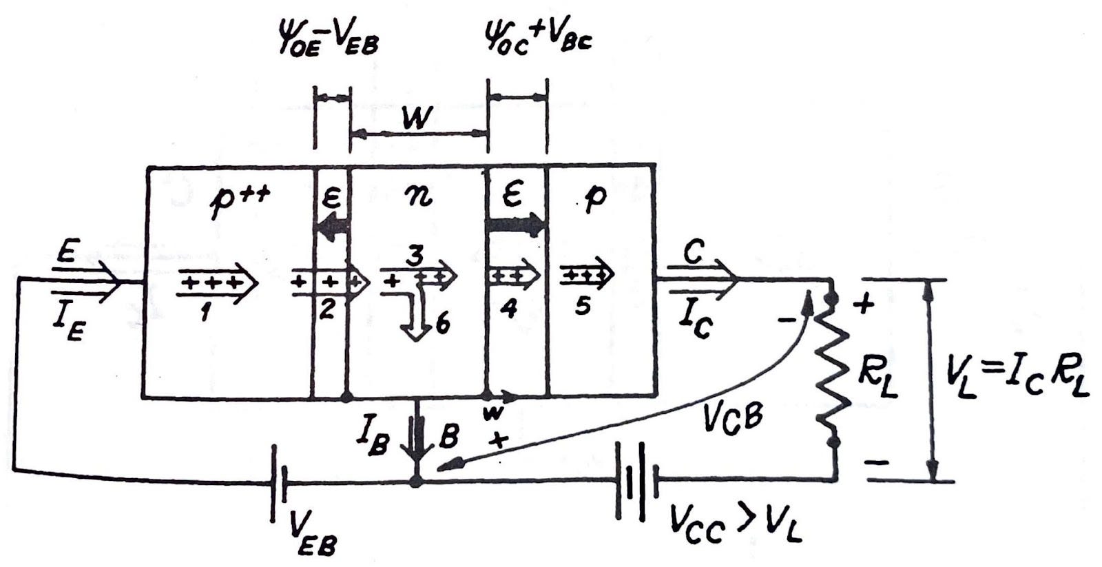
To understand the inner workings of a transistor of this kind, let’s assume a p-n-p arrangement where we forward-bias the emitter junction, that is, the positive terminal of the voltage source connected to the emitter, and the negative terminal to the base (see figure above). Conversely, we reverse-bias the collector junction: negative terminal of a power source to the collector, positive terminal to the base. This way, the emitter to base current is large because the junction is forward-biased—with the current value being governed by the diode equation. Given that this junction is highly asymmetric (the doping of the emitter p-region is orders of magnitude higher than the doping of the base n-region), the emitter current will be largely composed of holes going from the p-side to the n-side (current 1 in the figure). If the base width (W) is narrow enough, and because the base area is electrically neutral, the holes traversing through the emitter junction will find their way to the collector junction where the electric field will capture and inject them into the collector area (currents 3 and 4 in the figure). Some holes will recombine in the base (current 6), creating a base current which is very small due to the low doping of the base section and the small width of the base. With all this, the emitter current is passing almost unaltered to the collector. The collector current is almost independent of the collector-base voltage, as long as this voltage remains negative. Otherwise, the collector would also inject holes into the base, altering the overall functioning of the device. This is an important mode (saturation mode) we will talk about.
The electric field at the collector junction injects the holes into the collector area, and the magnitude of this electric field does not affect the amount of holes arriving to that place. It is the base and the diffusion that happens there which defines the amount of holes that will pilgrimage to the collector. Even zero volts between collector and base would keep that current flowing.
Thus far, we have been analyzing the behavior of the transistor mostly from its direct-current (DC) biasing perspective. The analysis to follow should be about observing how the transistor behaves while in the active region and when fed with small—and not so small—AC signals superimposed to base voltages, causing the device’s biasing to fluctuate around certain points, and how the input and output signals should match each other, minimizing alterations (i.e., distortion). Although understanding this is of great importance and a topic in itself which finds applications in a myriad of fields such as radiofrequency, communications, hi-fi audio and whatnot, for this discussion we shall focus on the device in switching mode, that is, moving between defined, discrete conduction states: from cut-off to saturation, and swinging between them as fast as possible. In this mode, the transistor acts as a switch, evolving from one extreme state (cutoff, or open switch) to the other (saturation, closed switch), and not caring about how similar the input signal looks compared to the output signal.
A transistor operating in the cutoff region has its two junctions working in reverse bias mode. In this situation, only leakage current flows from collector to emitter. Conversely, in saturation, the device has both junctions in forward-bias mode, allowing a small depletion layer and unleashing the maximum current to flow through it.
The transistor in switching mode sets the foundation of the underlying behavior of most digital electronics and computer systems out there.
So, all this hassle with electrons, holes, donors, acceptors and jealousy at Bell Labs only to create a switch? Really?
Yes.
But a very special kind of switch, one that would go down history to spark a revolution. The junctions we described above, in the form of diodes and transistors, would become the basic building blocks of our modern digital toolbox. A toolbox that supports today’s machine learning, artificial intelligence, cloud computing, but also Instagram, TikTok and the metaverse.
How?
Diodes and transistors would eventually form logic gates and memory cells. Gates would form flip-flops. Flip-flops would form registers, decoders, multiplexers, demultiplexers, adders, multipliers and full-blown arithmetic units. As integration technology and processes would mature, designers would start packing logic blocks such as memories, ALUs and buses inside smaller and smaller silicon bodies. Then, engineers would create a sort of digital machine whose behavior could be slightly modified—that is, perform different arithmetic operations or moving data between parts of its architecture—by means of binary words stored in a memory, giving way to CPU architectures, instructions and machine code. Corrado Böhm in his PhD thesis would conceive the foundations for the first compiler—which still lacked the name, with Böhm being one of the first computer science doctorates awarded anywhere in the world—an invention that would appear as a way of coping with the natural lack of human readability of machine code. The word ‘compiler’ would be coined by Grace Hopper, who would go and implement the first compiler ever. Thus, compilers would accelerate the process of facilitating the development of different run time behavior; what we now call software. In our eternal quest for more and more abstraction, and as different CPU architectures would appear, we would find a way of devising and pack layers of standardized software libraries and services that would dramatically ease our way of programming application software on top of dissimilar hardware, giving way to what we now call operating systems which would, in the process, make some people obnoxiously rich.
And as bipolar integrated circuits would pass the baton to more efficient foundry processes3, and as the physical lengths of integrated transistors would shrink and their density would double every 2 years, their power consumption and speed of switching from cutoff to saturation would continue decreasing and System-On-Chips, CPLDs and later FPGAs would come about, all combined with a new breadth of spectrum-efficient digital modulation and signal processing techniques, mobile devices would materialize, maturing with them important related domains and technologies like displays, allowing us to create arbitrary arrangements of pixels in screens whose colorful photons would hit our retinas, creating appealing user human-machine interfaces in applications that would allow us to, for example, send a poop emoji to a friend for comedic or illustrative purposes.
It all escalated quickly, and all happened roughly in the same timespan my dad has been alive.
Personally, I don’t like sand. It’s coarse, rough and irritating. and it gets everywhere. I also don’t like Star Wars references.
https://aip.scitation.org/doi/pdf/10.1063/5.0046150
https://www.nature.com/articles/442631a
Content has been adapted and illustration has been taken from the great book “Electrónica del Estado Sólido” by Ángel Tremosa
This process is actually based in metal–oxide–semiconductor field-effect transistor (MOSFET) which is a different kind of transistor compared to the BJT. MOSFETs have an insulated gate, the voltage of which determines the existence and conductivity of a conduction channel used for amplifying or switching electronic signals.